
GO Faster Go Further
Established since 2001

Hydrogen Hot Rodding™ ©

Secure Supplies Group


Stanley Meyer Maintaining Polarization


Yes this is Priceless Rare Data of Stanley A Meyer and Knowledge suggest you back up all of it immediately and share it to others.
After years over 20 years of Study on the Matter , we have found and seen that a spark gap with or with out a centre extract ground electrode( between gap centre sid of tube), contains all the frequencies in the spark event, this causes a auto resonance.
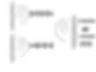
In Most of Nikola Teslas Designs the cold voltage comes from cycling 2 connected and osolating coils which when collapsing cause cold spark from center of coil for example a ignition coil is neither positive or negative.
It is our belief Stan was trying to do that with a solid state method.
it has been suggested that resonance can only oocur when consistant dbd barrier voltage is in place with pressure on the cell via cap, and gas present between electrodes causes a consistant state to tune to , some saying easy to tune air resonance rather than water?.
or can we learn from tesla?? sealed external spark gap with eec
Simple welcome to water fuel.
Here we show record and discuss the avoidance of grounding the dbd barrier
aka the helmholtz layer in the WATER fuel cell
circuit, and cell to maintain polarization state of wet cell with distalled water only and dbd barrier thinking as we do it..
UNderstanding this page and getting it to occur in a sustained way means you very very close to resonance and unlimited fuel and energy outputs as electrons are release from bond stored in the water and fuel gases become a bonus.
Start
There has been some discussion on where to place the probes on the VIC to take voltage measurements.
Why not use this method? It will give you the VL, VC and the VT across the choke and capacitor. Is that not what your really wanting to measure?
If you work out the formulas Stan gave you, you want even have to probe it, the formulas will give you the answer your seeking without a probe.


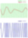
I would like to open up a discussion about two photo's below. I want people to post and explain their comments about the difference's they see in the two photo's.
Let's look at what is going on in those two photo's.
In photo one, You will see most people using this photo even after I have told them many times to stop throwing high voltage to the cell.
For that is all they are doing and it will not create any gas.
The only way you will ever create any gas with high voltage with photo one is using it to Fracture the water molecule like in the injector.
And it will take more high voltage than a copper coil will ever produce. This is exactly what people like Ed M. is doing.

In the Pict.2 you will see a constant high voltage, from 0v to Va.
You never want the voltage to fall below this voltage because it sets up the polarization process and low gas production and it can never be lost.
As you can see this is a constant pulse voltage with no gating at all. You can see this in Pict.3

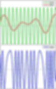
Now this is where people have been getting all this wrong all along
Stan states to superimpose a gating signal onto the pulse frequency.
Most people is killing the polarization process with the gating because they are using Pict.1.
Now let's add the gating to Pic3 below . without increasing the voltage this is what you will get.
Do you see the gating in Pic3 below ? It's there trust me it's there, I added it. LOL

Now let's increase the voltage from Va to Vn.

The old saying goes, it takes money to make money.
Same goes For Stan's way, It takes gas to make gas.
So are you saying the voltage shouldn't be completely shut off during gating?
Exactly, If you shut the voltage off completely you will never create the polarization process and keep it going.
The polarization process can't be created on the fly like in Pict1 using high voltage.
How do you keep the circuit from not shutting off during gating?
From the looks of Stan's circuits it seems like they shut off completely during gating.
The only thing I can think of is maybe the gate frequency has something to do with it?
I had to build a circuit to do it. But with Stan's GMS and VIC cards it will do it all for you.
But I will tell you the gating frequency and the pulse frequency has to synchronized with each other.
Stan does this with his frequency card. All the frequencies that come from his main frequency card is all synchronized with each other.
Just build yourself Stan's frequency card and build yourself an offset circuit for the gating frequency.
That doesn't make sense to me, unless there is something I am not seeing in his diagrams and PCB's.Which frequency card are you talking about, the gated pulse freq gen or the variable pulse freq gen
The main frequency generator board.The gate board is for the GMS unit that controls the gating for the Digital control means card.
All you will need is an offset circuit for the gating frequency.
You can find one in Stan's circuits. There is one on the voltage control card and also on the Vic card. I'm sure you can find a simple offset circuit on the web.
It's just an offset that raises the gate signal above 0 volts to 2, 3, 4, 5 volts above ground state, so the polarization once created can't be lost. When Stan say's the process starts all over again, He don't mean from ground state.
an you point it out in Stan's circuits....That's something I've never noticed before.
From what I just looked at it's part of the 741 op amps Stan used?
It is part of the 741 op amps.
This is just one example of offset and gain control.
If you look at the GMS and Vic unit all the offsets and gains has lock nuts on them so they can be set and never be moved once set.
If you look at the Accel card on the GMS unit you will see low idle and Max that is also offset and gain controls.

VERY IMPORTANT
Wow, that alone is probably what has stopped so many of us from
getting the cell working. Thanks GPS
The only issue it's going to cause is if you don't have it right you'll saturate
the core.
You want saturate the core if you pick the right core for the frequency you will be pulsing at.
Here is a couple things that may help you understand better also.

t does make sense as it keeps the molecules aligned during the "off time".
I looked into dielectric relaxation years ago but never connected the dots...
Exactly, as long as them little molecule's buggers are spinning you will never stop them long enough to align them to make any gas using Pic1.
By the time you get them to slow down your letting them spin again. :)
Your last string of posts have made it absolutely clear to me why you chose to use Stan's exact circuits.
There was no way you could have known what to do until you actually saw Stan's circuits doing it. Thank God you listened to your gut on this one.
Also, great detective work reverse engineering Stan's circuits.
Looking at the Voltage Amplitude Control, is producing 2V to 9V feeding the tx of the primary.
The offset and gain, control the 2V offset and gain the speed it will adjust the voltage depending on the input (J) pulse frequency from the accelerator card
If we were to build the opamp schematic what signal do we need to feed on J'' conection without building the digital control means,analog voltage gen.because they are tided together.
Right once again about the freq of the gate.the variable freq gen sets up the freq of the whole gated signal,but works only on two setings if you go up in freq the 74122 is not reacting.


Since most of us are not building the whole GMS unit there is no need to superimpose the two frequencies is there? No need for the 4001 NOR gates.
All we need to do is use the gating circuit to control the voltage amplitude.
Then the pulsing circuit can control the switching. Makes things easier in a way.
I have created the offset circuit and put it on the gate frequency coming off the K2 card, going into the K3 card at B/AUTO.
Testing the signal output of the offset circuit I can see the gate frequency elevated off 0. But, when the two frequencies are mixed by K3 card I'm not seeing it from the output of A.
I interpreted you to say that it should be added to the gate frequency. Am I placing the offset circuit in the correct place?
Just like Stan did once you get the GMS and VIC circuits worked out you can have it all put on a microcontroller.
Stan worked with a company years ago to have the controller chip built, he actually had a few of them made I believe.
I contacted the company a few years back and it's no longer in business. Tried to get in touch with the people who worked on the project and got in touch with a few of them.
Unfortunately all the info they had was discarded as for them it was just another project. They did tell me it was a circuit to control the system but was mostly used to control the pulsing of a complex laser injection system in which Stan would expose the water to high power laser radiation...
Just got my new scope today, awaiting my new dual channel freq gen and some other equiptment....Hopefully testing will start again in a month or less.
Does your dual frequency counter have offset control on it?
Also check it and see if both frequencies are synchronized with each other.
==========================================
Yes and it also has a sweep function.
I can sweep over any amount of frequencies I choose for a time period of up to ten minutes.
I can also control it with my computer....pretty excited to get it and start playing.
Not sure of they are synchronized though....that might be a problem....I can adjust the gate duty cycle to match the end of the resonant pulse frequency, might be tricky though....
How closely do they have to be synchronized?
What exactly do you mean by having them synchronized.....How is that done when the resonant frequency changes?
Some people has looked at my sperm wave and made comments about it.
For some reason they must have not read the first few pages of the Tech Brief where it states.


So, it's an amplitude modulated wave???
The resonant freq is the carrier while the gate is the modulating wave?
Stan led us all to believe he was charging the capacitor to a high DC voltage?
I still don't get Stan explaining the choke as a pfn,
it discharges right when the applied pulse ends.
I guess you could call it a pfn but an inductor does the same thing....
Perhaps this might help?
http://www.angelfire.com/moon2/xpascal/MoonHoax/ApolloSystems/ApolloSystems.HTM
The following sections are authentic and can be found
in the Apollo handbook found on the NASA site; here is the link:
Link to the LM handbook
I) THE COMMUNICATIONS SUBSYSTEM OF THE LM
In this section, I am going to talk about the communications subsystem
of the LM as it is described in the LM's handbook.
I'll first talk about the way received signals are separated.
Low frequency signals can't propagate all alone though space; their low frequency makes them unfit for that purpose.
On the other side, high frequency signals are able to propagate, but their frequency is too high to be audible.
So how is this dilemma solved?

This problem is solved by modulating a high frequency signal, called the carrier, with the low frequency signal which contains the relevant information (voice or music for instance).
The carrier has a high enough frequency to propagate through space.
There are several type of modulations:
1) the amplitude modulation consists in changing the amplitude of the high frequency carrier according to the low frequency signal.
This was the first type of modulation used.
However, this type of modulation can be a little affected by noise.
2) The frequency modulation consists in slightly changing the frequency of the carrier according to the low frequency signal.
In this type of the modulation, only the frequency (slightly) changes, but not its amplitude which remains constant.
This type of modulation is more immune to noise than the previous type, and gives a sound of excellent quality.
However the range of propagation is diminished comparatively with the previous type of modulation, and needs more relays.
The phase modulation consists in modulating the phase of the carrier according to the low frequency signal.
Like in the frequency modulation, the amplitude of the carrier remains constant.
The phase represents the time that a period of the wave starts.

For instance, the two signals I represent here are in phase.

And the two signals I represent here are dephased of 180°
.jpg)
But a receiving antenna can receive several signals emitted from different sources, and contain different informations which must be separated and received independently.
So, how is this separation made?
When two independent sheathed wires are are wound around a common core, if a variable current is applied on one of the wires, then this variable current is also found on the other wire, although there is no direct electrical contact between them.
That's called magnetic induction.

So, if we send our high frequency signals on one of the coils, we'll also find these signals on the other coil.
But you'll say that we still haven't solved our problem of signal separation, for the two signals are still mixed on the other coil.

Yes, but if we apply a capacitor on the two ends of the other coil, then the signals are stifled on the other coil.
Well, we now have stifled both signals, it still doesn't solve our problem of signal separation.
But in fact, it does, for if we apply a capacitor on the ends of a coil, that we load the capacitor with a battery, and then make it discharge through the coil,
there will be the creation of an alternating current of a given frequency which depends both oh the inductance of the coil, and the capacity of the capacitor; this frequency is called resonance frequency of the LC circuit.

If if is not easy to make the inductance adjustable, it's different with the capacity of the capacitor.
It's possible to make the capacity of a capacitor vary with two sets of metallic plates which pivot relatively to each other.
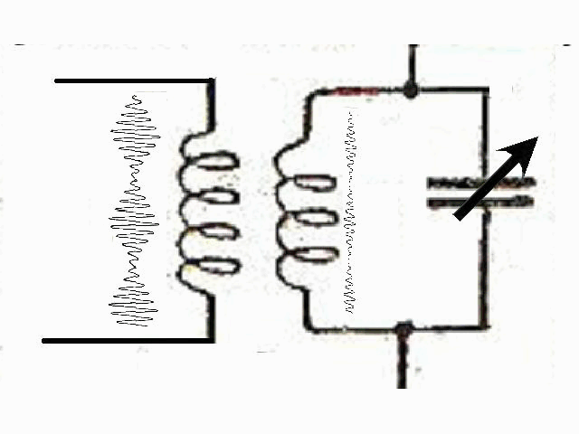
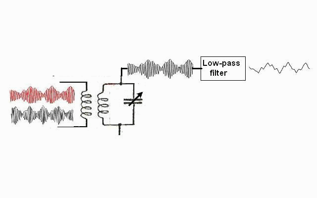
If we apply a high frequency signal of the first coil and a variable capacitor is applied on the ends of the second coil, the signal which appears on the second coil will be stifled, except when the capacitor is adjusted so that the resonance frequency of the LC circuit matches the frequency of the signal which is applied on the first coil.
Given this property, it then becomes obvious how the variable capacitor allows to separate the two incoming signals:
When it is the first signal which is to be selected, the capacitor is adjusted so that the resonance of the LC circuit matches the frequency of the first signal, and conversely, when it is the second signal which is to be selected, the capacitor is adjusted so that the resonance of the LC circuit matches the frequency of the second signal.
You'll say that the carrier which is obtained on the second coil is still a HF signal which is unfit for being listened to, but this carrier can easily be eliminated by a low-pass filter which lets only pass the low frequency signal which may then be listened to, after appropriate amplification.
You may point out that one of the modes of modulation
I described uses frequency modulation, and wonder if, when the frequency varies, the signal is not stifled by the RC circuit along its variation?
No, in fact, for the variation of the frequency is slight and allows the signal to be accepted and not stifled by the LC circuit on its whole range of variation.
The radioreceiver that I show here is of course much simplified, and just purposed to give an idea of the way it works.
This mode of signal selection of course supposes that the two signals use carriers of different frequencies.
The separation of the signals would not be possible if the two carriers were using the same frequency.
That's why it is absolutely mandatory that the radio stations all emit on different frequencies.
Two radio stations which would use frequencies which are identical or too close would not be clearly heard, and each one would be a cacophony to hear.

What is also frequently used in electronics is a crystal oscillator which allows to obtain a very stable frequency which does not vary.
An electronic circuit allows to produce a variable current of a given frequency which depends on the adjustment of this circuit.
When a special device, called "crystal oscillator" is inserted in this circuit, it forces the oscillator to have a very definite frequency, which is extremely stable and shows no (or a negligible) variation.
I must also have some words on the radar.
A radar sends a wave to space; when the wave bumps on an object, the wave comes back to the radar; the radar then knows it is pointing at that object, and by measuring the time between the emission of the signal and its reception, it can know at what distance the object is: Indeed, knowing the speed of propagation of the signal (the light speed) , it is possible to convert the travel time of the signal into a distance.
Generally the signal of the radar just bumps on the object it tracks.
But in some case, this object may be an intelligent object (such as the LM) which is equipped with a transponder.
A transponder is a device which retransmits the signal it receives.
The advantage of this is that the radar will receive a signal which is cleaner and stronger than if the signal was just bumping on the object.

Now, if the signal sent by the radar was continuous, it would not possible for the radar to know when started the signal it receives, and so it would not be able to determine the travel time of the signal.
That's why, instead of sending a continuous signal, the radar sends instead bursts of the signal separated by silences.
That way, when a burst comes back, knowing the time that the burst started, the radar is able to measure the time between the emission of the burst and its reception.

Eventually, the transmitted signal may be continuous when it is retransmitted by a transponder,
but in this case it contains information which gives timing indications; here I show this signal modulating the carrier in amplitude because it is easier to represent, but it more generally modulates the carrier in frequency (or phase). continued here
BTW, when I modeled and simulated the VIC in multisim a few years back I added in the capacitance of the chokes. Once I did this I simulated the circuit and guess what happened? I got an Amplitude Modulating waveform! Maybe that is why Stan talks about the coil capacitance as if it's so important. In that circuit the resonance was occurring between the choke and the cell, but the chokes themselves also formed a parallel LC circuit which caused the voltage across the cell to change polarity, even with the diode in the circuit the choke capacitance makes it possible.
I've been reading up on modulating rectors. If the L1 choke is a modulating inductor then somehow it plays a role in determining the gate (modulation) frequency...This is where I get lost.....I am also not understanding how the modulating frequency passes through the circuit, it should be impedance matched somehow or else the circuit would reject it because of it's high Q factor?
Is the modulating (Gate) frequency a harmonic of the carrier (resonant) frequency?
I know you said the two must be synchronized, I'm just trying to understand why?
If you look at Stan's schematics,
on the digital control means schematic and the analog generator you will see rising edges and falling edges signals with Dots on them.
The dots tells you if the signal is on the rise or on the fall edge. In the photo below tells you it cares less what the rising edges is doing or when it occurs,
it only cares when the falling edge occurs. That's how he is able to keep everything synchronized, some IC chips works on rising edges and some work on falling edges.
So the falling edges of the pulses are synchronized?
Thinking about the circuit I'm sure it's synchronized so that the resonant pulses aren't cut short...if so that pulse would have a different frequency and might throw off the whole impedance of the circuit.
Couple good videos on the VIC Card and how it works. May want to take a look and get busy, they finally got it to work .
There are 2 obvious annotations
1. the frequency lock in mechanism shown in the video to a given frequency from the generator
won´t work in Stan Meyer vic/wfc operations mode.
Why? because Stan´s feedback signals dont´t give a frequency return but a phase shift information. the feedback frequency is ALWAYS identical to the vco out frequency but phase shifted and vco adjusts frequency until phase shift needed is reached. in the video phase shift is 0° but that´s not the phase shift condition needed in Stan Meyer´s vic/wfc system
so this video shows a wrong understanding of what´s going on in Stan Meyer´s system and what´s needed from the vic card.
they would have noticed that their circuit doesn´t work as needed if they had used a tank circuit (lc-circuit) instead of a function generator as I did in my pll operations demonstration at
that video shows real life feedback signals as returned from a vic/wfc combination.
With that kind of a tank circuit you can create phase shifted return signals at identical frequency like vco out with phase shift.
2. to "optimize" the lock in feature by cutting off one of two phase shift indicators is also wrong understanding. now you have a pretty shiny led lock in but for the wrong condition :(
... and wait a moment ... "duty cycle is not always 50%" is an interesting statement, but cutting off one of the indicators to get rid of the "problem" is also wrong understanding.
So this vic card does something similar to a vic control card needed but something different and it can´t operate vic/cell in Stan Meyer operations mode. Sadly it can´t be tested or "optimized" until a fully operational vic/wfc combination is connected. And there is no fully operational vic/wfc combination out there.
If you ask why Stan implemented scanning mode and pll lock in switchover the answer is that CD4046 can´t lock in if frequency is too far away from frequency where phase shift is 0 or 90°. so for a startup condition he has to scan until reaching frequency ballpark and then switch over to pll mode. further phase changes will be adjusted by pll vco without further scan as long as pulsing continues. Once pulsing stops for whatever reason system has to re-sync to given phase shift or worse restart in scanning mode.
State-of-the-art pll control could immediately start in pll adjust mode without any scanning and as long as there is no fully operational vic/wfc combination running it would be beneficial to adjust to any phase shift beween 0 and 179° as needed. CD4046 can´t do that at all!
I'm not sure why they modified the board. I am 100% sure you would not have to modify it as long as it works and scans in the frequency range for a 10 cell unit. In my case used with a 6 cell unit, I know what frequency it operates at and may have to modify the range it scans. Other than that It should work just fine the way it is. Will let everyone know soon.
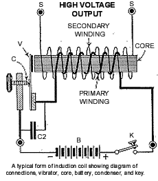
Can anyone here tell me what diode Stan used in line with the primary coil, the 5kV 1A one?
Not 100% sure but 99.9% it is a 1n5408 3amp 1000V
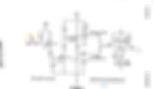
I made a group of pics so we can see beter.The digital control(has acceleration circuit on it) is tided to the analog voltage gen.then that goes to amplitude control,so...they all tided.I searched all the opamp circuits,i built stan's sch.but it only controls the ON pulse up and down.You cannot control 2 freq.with a single output of an opamp.the signal must be fed to the opamp inputs +,- to controll its offset
HMS-776, in pin 2 of the opamp there is not a square wave,but i think you place that to experiment.If we trace back the schematic we can se that on analog voltage gen there is another offset opamp,and before that there is a manual speed calibration which is a pot as a voltage devider,thats where the signal starts,excluding the digital control.And from what i saw in all schematics ''VDD'' is 5v, VCC is12v.

Yeah that frequency to the 741 pin 2 represents the gate frequency. You see in the waveform when the gate is "off" the voltage across the resistor (primary coil) decreases but does not go to zero. The amount of offset changes when you adjust the pot.
From GPS's explanation that's what I understand the circuit is supposed to do and the simulation shows the same thing....I just picked out all the other stuff as I am not building the whole GMS unit, I just want to get my cell working....I think I need to do more work on the offset circuit though as right now it's just not giving me a wide range of control.
UPDATE, I kinda figured I was doing something wrong in my multisim simulation of the offset circuit and I found the problem. I was just using the wrong pulse supply, I think it was only supplying 5V and it's not adjustable.
The pic below shows the working offset circuit. I might play around with it more later and try to get more adjustability out of it. For now the offset goes from 8.43V to 9.15V peak and can be adjusted down to as low as 80mV to 9.15V peak! The effective range of the pot is only from 5%-50% but it works. Pictures below show maximum and minimum offset. final in modern circuits
If you go below 5% or above 50% your peak voltage and offset drops sharply.


