
GO Faster Go Further
Established since 2001

Hydrogen Hot Rodding™ ©

Secure Supplies Group
GMS UNIT ECU EMS
STANLEY A MEYER


HIL ( Hardware In Loop TEST Bed, ECU Prep System)
Why Test ECUs with Hardware-in-the-Loop Simulation ?As software explodes in complexity and size, comprehensive ECU tests are necessary more than ever before. Only a tough zero-error policy can help avoid vehicle recall campaigns. So for many manufacturers and suppliers, ECU testing has become a key phase in the development process. However, real test drives are expensive. They often take place in the freezing cold or the searing heat to test ECUs in extreme conditions. You also have to contend with the necessary vehicle prototypes not being ready on time, so testing is delayed. Simultaneous engineering, in which development processes run in parallel, can be difficult to achieve. These are just a few of the problems inherent in real test drives. Not only are the drives themselves dependent on the weather and on vehicle prototypes; test engineers face actual physical danger and have to cope with incomplete test results – not to mention the immense costs in terms of time and money. The solution: virtual test drives within a hardware-in-the-loop simulation environment.
GMS Parts
for Sale here

Whats the Diference between this and Exisiting Car Ecu's and Systems?
Not Much Basically we use the same test bed system taday as Stan Did, if fact stan purchased his and adapted it with his hard card so we can too. The System for Bench testing circuits and than flashing ECU's for install is call HIL ( Hard Ware in the Loop) When Stan did it he had no internet and no software or decent pc. These Day HIL system have pc built in and connect to web !
So what do we need to add or make the LPG Style Piggy Back Ecus Do? We we test in that HIL way?
1.We add some new In out accessories for the EUC to Control.
A. We instruct Ecu to send out a Signal from the Accelerator Thottleposition sensor to be mirror
and or have a coresponding Scaled Frequency Duty and and Pulse duration signal
similar to the speed increase signal to each injector. This goes to our New pc of Equipment (card)
or chip functioncalled frequequency Generator, (which will send the desire rate width ad gate of
frequeceny at a certain speed to our Electroluzer Cell Transformer + VIC Circuit ( Voltage Intensifier Circuit).


Complete Library of Assembly Manuals
Price $595. for ALL MANUALS
Availability PDF format - immediate download
Complete Library of Assembly Manuals
Priced $595
Buy Now Individually !!
NEW Guide Books Each Circuit in GMS
If you are not currently in a position to purchase any of our Experimental Generator Kits,
but would like the opportunity to learn about the mechanical construction or electronic circuitry in advance, or for educational and/or personal experimentation purposes,
this will be of great benefit to you.
Comprehensive Assembly Manuals Include:
-
Exploded View Mechanical Drawings with Numbered & Descriptive Itemized hardware parts
-
Complete Electrical Wiring Schematics
-
Illustrated Diagrams
-
Photos
-
Construction & Operation Tips
-
Includes NEW GMS Assembly Manual
All Assembly Manuals are Copyright © Secure Supplies, and are NOT for publication or document retransmission in any form.


Digital Book

Digital Book

Digital Book


The is From the Technical Brief & control & driver circuits patent .
The following info: Refer to Tech Brief Figures 3-2, 3-4, 3-5, 3-6 and Patent WO 92/07861
GMS CARD DSCRIPTION CIRCUIT PRICE
-
Circuit K6=? (Checking if Gas Feed Back Card)
-
Circuit K7=Laser Accelerator/Distributor Optoschmitt (Photodiode) $80
-
Circuit K17=?Circuit K18=?
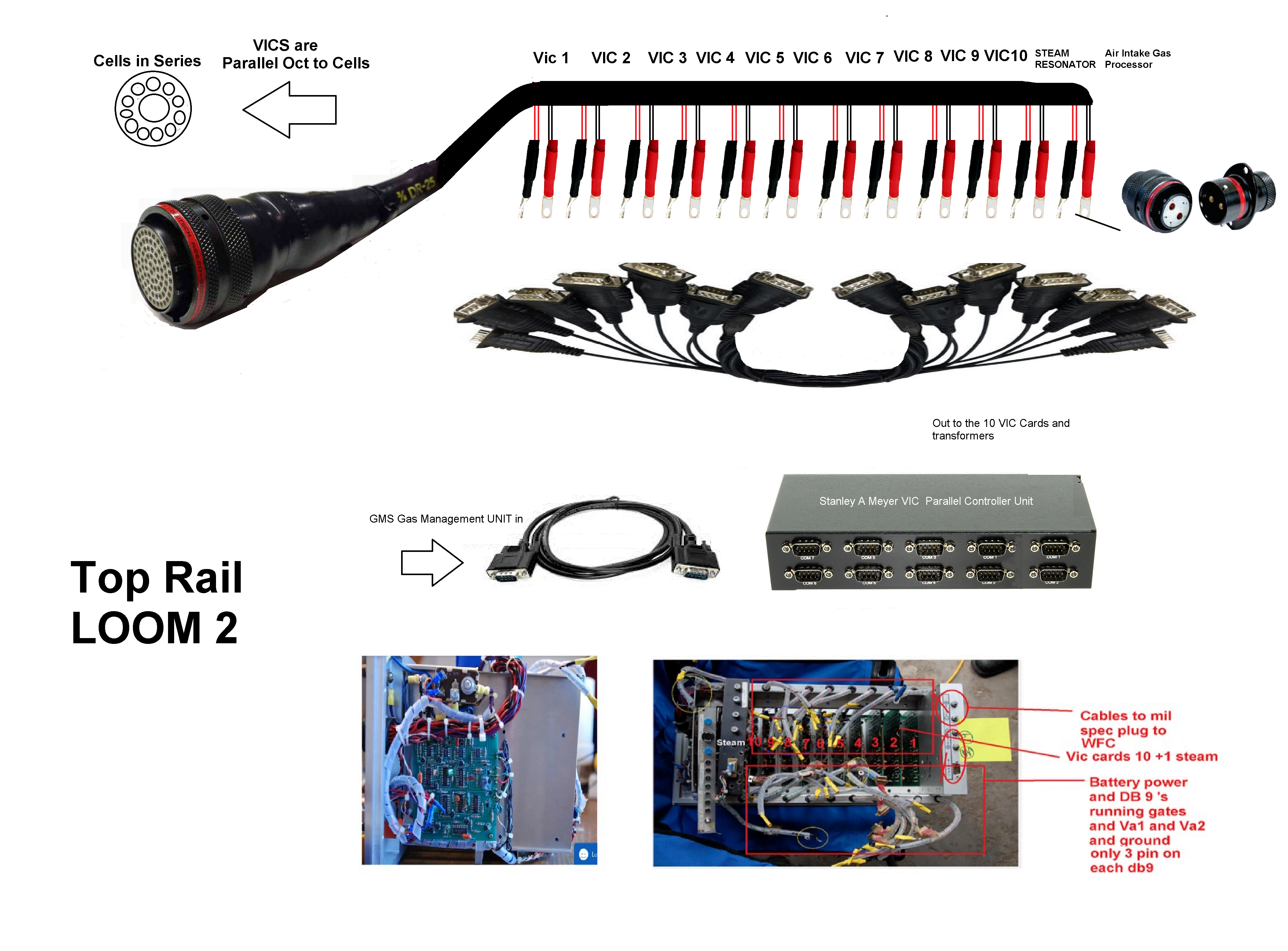
VIC Cabinent ( BOx) in the VIC cabinet there were two other circuits,
one for the "Steam Resonator" and another for the "Gas Processor".
GMS Box (Box Only ) No Cards Spcial Order $500
Buy all Blank Circuit set inc 9xa 9xb scr epg alternator $800

Stan had a card extension board that would plug into any card slot to allow the main card to be extended outside the box to tune any on board internal pots or adjustments.
Once the card was properly tuned and or adjusted the card was removed from the card extension and placed back into it's slot and the card extension was placed back into It's slot.
The card extension was designed for anyone of the cards to be removed and plugged into it and it still function outside the box.
We will not be using the card extension in our design. Nor will our boards plug into a back plate,
They will have plugs with extended wire in order to get the boards outside the box for adjustment.


All ECU
now have
this 1.
All ECU
now have
this 1.
All ECU
now have
this 1.
All ECU
now have
this 1.
All ECU
now have
this 1.
All ECU
now have
this 1.
Add to ECU
Add to ECU
Add to ECU
To See each card circuit Circut in Detail Click Scroll Down

All ECU
now have
this 1.

All ECU
now have
this 1.

All ECU
now have
this 1.

All ECU
now have
this 1.

All ECU
now have
this 1.

All ECU
now have
this 1.

All ECU
now have
this 1.

All ECU
now have
this 1.

GMS and VIC Toggle Switches and Color Caps
These look like they would duplicate the switches in the Gas Management Unit, and the VIC cards. You can even just buy the colored caps.
http://www.amabilidade2002.com/onoffswitch5.htm
GMS and VIC Toggle Switches and Color Caps
Here is another from Jameco, but with a black cap.
https://www.jameco.com/webapp/wcs/stores/servlet/Product_10001_10001_75951_-1
Circuit Card L1=Variable Pulse Frequency Generator (Circuit K2)Card
-
L2=?Card
-
L3=Gas Injector Card (Circuits K10, K13)Card
-
L4=Gated Pulse Frequency Generator (Circuit K3)Card
-
L5=Acceleration Card (Circuit K11)Card
-
L6=Dual Regulated Power Supply (Circuit K16)Card
-
L7=Gated Frequency Oscillator (Circuit K15)Card
-
L8=Laser Distributor Optoshmitts (photodiodes) (Circuits K7, K12)Card
-
L9=Safety Control Circuit (Circuit K1)Card
-
L10=Laser Accelerator Optoschmitts (photodiodes) (Circuits K7, K12)Card
-
L11=Analog Voltage Generator (Circuit K8)Card
-
L12=Voltage Intensifier Control (Circuits K4, K5, K9, K14, K21, and the EEC per Fig 3-2 Tech Brief)
I need help as the list is not complete. I have not determined what circuits K6, K17, and K18 are.
I have not determined which circuits are on Card L2.
And I have not determined which Card(s) the following circuits are on: K6, K17, K18, K19, K20.
I know of one cirucit for sure which is missing and it's probably K6, K17, or K18. That is the Gas Feedback Control Circuit (Figure 11) from the Control & Driver Circuits patent WO 92/07861ali: Circuit
-
K1= Figure 11 - Safety Control Circuit (L9)Circuit
-
K2= Figure 12 - Variable Pulse Frequency Generator (L1)
-
Circuit K3= Figure 6 - Gated Pulse Frequency Generator (L4)
-
Circuit K4= Figure 5 - Cell Driver Circuit (L12)
-
Circuit K5= VIC CARD - Voltage IntensifierCircuit (L12)
-
Circuit K6= ?
-
Circuit K7= - Laser Accelerator (only) (L10)
-
Circuit K8= Figure 3 - Analog Voltage Generator (L11)
-
Cirucit K9= Figure 4 - Voltage Amplitude Control (L12)
-
Circuit K10= - Injector Circuit (L3)
-
Circuit K11= Figure 2 - Digital Control Means (Accel) (L5) IMPORTANT
-
Cirucit K12= - Laser Distributor (only) (L8)
-
Circuit K13= - Gas Injector Circuit (L3)
-
Circuit K14= Figure 9 - Pulse Indicator Circuit (pulse pickup) (L12)
-
Circuit K15= - Gated Frequency Oscillator (L7)
-
Circuit K16= - Dual Regulated Power Supply (L6)
-
Circuit K17= ?
-
Circuit K18= ?
-
Circuit K19= - Exhaust & Air Gate Control Circuits
-
Circuit K20= - Summing Circuits
-
Circuit K21= Figure 7 - Phase Lock Loop Circuit (L12)
-
Circuit K22= Figure 8 - Resonant Scanning Circuit (L12) 8)
Quote from: Dynodon on April 17, 2011, 15:38:21 pm ---Just forget about the last C circuitAli, all the circuit boards are labeled with the K1-K21Don--- End quote ---PSfigure 7 refers to K22 which is Figure 8...
also, the WO92/07861 is not all correct... and also, in the Full Data From Estate, there is schematics from the WO92/07861 with component values...
Analogue Connection Box ,
The Modern version is Can bus

1) Alarm (7 pins)
2) Dist (7 pins)
3) Gate (2 pins)
4) Accel (32 pins)
5) Exhaust Gate (2 pins)
6) TOR (8 pins)
7) DC Power (2 pins)
8 ) VIC Circuit (6 pins)
The GMS Unit connected to the
Voltage Intensifier Unit.


Digital Control Means
and Anologue Voltage Daughter Board.

Note 2023 From Earl
This part you mention is some thing I have not studied on this topic but it now makes me think wow if that is true. You stated
Interesting so the duty cycle on throttle and digital means boards is used by analog board to set voltage level. It also goes to gate board to sync both signals and you use the gate board to set duty cycle of gate to 90 percent using the pot on the gate board.
If I remember correctly the gate board uses the OR logic to set length of duty cycle. I will double check this however this means you would need to not let the duty cycle of pulse from the throttle board exceed 90 percent. This could explain why the digital means and throttle board interface is wired the way it is.
Note: I did some tests on the gate board and frequency of gate only changes very slightly with frequency of input and this was over large changes of frequency i.e. 50 to 5K.


Stanley A Meyer Anologue Voltage Generator K9 here is the card that Piggy Backs thee Digital Control Means


Gates Pulse Frequency

So to be Clear the Digital Control Means has 2 Boards they are both for sale above


Digital Book


Stanley Meyer Injector (1 - 4) Control Circuit GMS 1


Stanley Meyer Air Gate Control Circuit GMS Font


Stanley Meyer Speed Limit Control Circuit GMS


Stanley Meyer Exhaust Gate Air Gate Circuit GMS


Stanley Meyer Alarm Control Circuit GMS


Stanley Meyer Voltage Regulated Power Supply Circuit GMS


Stanley Meyer Air Gate Control Circuit GMS


Stanley Meyer Distributor Control Circuit GMS 1 Stanley had 2 boards that is wwhy 2 shown here


Stanley Meyer Gas Feedback Control Circuit Back View GMS
This Unit will provide


The Voltage Intensifier Box Unit
This was Connected to the Main HIL Unit (GMS Unit) With a Cable. Basically this are Voltage Amplifiers 1 for Each Cell. They Whre Switch by a Common
PWM Circuit in the HIL ( GMS Unit)
Also in this Boax was a Voltage Controller for the Steam Generator (Water Heater)
and a Volatge Controller for the Air in take Ioniser (oxygen Prosessor) ( Gas Processor)


The Voltage Intensifier Rack Multi Transformer Rack
This rack contains 11 module cards
and a cable connection bay with 12VDC rail terminals,
2 cable connection ports and a power switch.The card modules are (from left to right):
1) Steam Resonator
2) Resonant Cavity 10
3) Resonant Cavity 9
4) Resonant Cavity 8
5) Resonant Cavity 7
6) Resonant Cavity 6
7) Resonant Cavity 5
8 ) Resonant Cavity 4
9) Resonant Cavity 3
10) Resonant Cavity 2
11) Gas Processor
Each of these cards have identical user interfaces.


Stanley Meyer The Voltage Intensifier Unit


Stanley Meyer The Voltage Intensifier Unit Ferrite Ceramc Core and Copper Coils


Stanley Meyer International Patent WO92-07861
Meyer’s International Patent WO92-07861 is a document that rises very nearly to the level of full technical disclosure with respect to his Hydrogen Gas Management System (GMS) and the sustained operation of the Electrical Polarization Process.You may obtain a copy of this patent from my server at URL:http://www.singularics.com/docs/meyers-WO9207861A1.pdfIn figure 1 below, Meyer lays out his system in an overview with the following coded block sections (listed below in sequence of operation).


The Hydrogen GMS also has the ability to apply dynamically generated voltage pressures to the collector of the FET that drives the VIC TX1. This functionality is provided by the Voltage Amplitude Control Circuit (fig. 4) and whose logic is managed by the Digital Control Means Circuit (fig. 2).
—– (Primary side of Tx) —–1 — Analog Voltage Generator Circuit (see circuit in Figure 3)2 — Adjustable Frequency Generator (see circuit in Figure 12)3 – Digital Control Means (see circuit in Figure 2)4 — Voltage Amplitude Control Circuit (see circuit in Figure 4)5 — Adjustable Gated Pulse Frequency Generator (see circuit in Figure 6)6 — Phase Lock Loop Circuit (see circuit in Figure 7)7 — Resonant Scanning Circuit (see circuit in Figure 8 )8 — Cell Driver Circuit (see circuit in Figure 5)9 — TX1 (see circuit in Figure 10) —– (Feedback from Tx) —–10 — TX3 (see circuit in Figure 10)11 — Pulse Indicator Circuit (see circuit in Figure 9) —– (Feedback from Resonant Cavity) —–12 — Gas Pressure Sensor (see Resonant Cavity in Figure 10)13 — Gas Feedback Control Circuit (see circuit in Figure 11) —– (Secondary side of Tx) —–14 — TX2 (see circuit in Figure 10)15 — TX5 (see circuit in Figure 10) to B – (connection to ground on Vss terminal o16 — Resonant Cavity17 — B+ to TX418 — Blocking Diode I have included below the referenced circuits listed above.You will also notice that Meyer uses letters A, B, E, F, G, H, J, K, L, M and M1 to indicate signal interchange (communication) between the various circuit elements. I refer to these as COM stages in what follows (eg. COM A, COM M1, etc.).The electrical energy for managing the waveform and also driving the resonant cavity fuel cell is supplied by the Analog Voltage Generator (fig. 3).

With access to battery power and with the system turned on, the first thing Meyer’s Hydrogen GMS must do is to determine the resonant frequency for the resonant cavity.This job is performed by the Variable Pulse Frequency Generator (fig. 12). It accomplishes this by interpreting a resistor based impedance matching network indicated in the “Pulse Frequency Control” section of the schematic.

The non-gated resonant frequency is then setup by the Digital Control Means circuit (fig. 2) through COM G.

The Digital Control Means circuit has two main jobs:1) Sets the required gate frequency given the degree to which the throttle is engaged. A high throttle setting corresponds to a shorter gate frequency which yields higher fuel gas output to accommodate the higher energy requirements of acceleration. This throttle dependent gate frequency is communicated to the Adjustable Gated Pulse Frequency circuit (fig. 6) through COM M1.2) Sets the DC voltage in the Voltage Amplitude Control circuit (fig. 4) through COM M. The variable DC voltage applied to VIC TX1 servers as a further control for governing the magnitude of the high voltage pulses that the resonant cavity experiences.

The Adjustable Gated Pulse Frequency Generator (fig. 6) produces the required gate frequency and combines it with the resonant frequency in real-time which it then sends to a Phase Lock Loop Circuit (fig. 7) through COM A.The Adjustable Gated Pulse Frequency Generator also adds one further tuning parameter to the gate frequency requirement – that of fuel gas pressure in the resonant cavity enclosure. The system uses gas pressure maintenance as part of the equation for calculating required gate frequency and DC voltage amplitudes that will enable the cell to keep up with the fuel demands of the engine. Gas pressure is constantly monitored by a gas pressure sensor which sends data to the Adjustable Gated Pulse Frequency Generator (fig. 6) through the Gas Feedback Control Circuit (fig.11) by way of COM K.

IMPORTANT NOTE
9 OUT OF 10 OF ABOVE DONE BY MUTLI STAGING ECu INJECTPR CONTROLLERS A INJECTION CONTROLLER , AFTER MARKET WITH 3-4 ROW INJECTION( 4X 8 INJECTORS FOR V8) EXAMPLE DRAG RACING . cHECK jegs ONLINEWITH A LITTLE MODIFICATION i FEEL IT IS CLOSER THAN WE THINK. PS NOW ECU ON ,
MADE IN CHINA .COM AND PARTS SENSORS ETC , HAVE AIR INTAKE BODIES ELECTRICAL CONTROLLED ( SO AIR GATE AND EXHUAST GATE CAN BE CNOTROLLED , AIR TEMP, PRESSURE IN SIDE OUTSIDE AND HUMIDY SENORS IN CYLINDER ALL OFF THE SHELF@!!SO WHAT IS LEFT? FROM ABOVE SOME LED'S?


Variable Pulse

Variable Pulse


Variable Pulse


Variable Pulse


Variable Pulse


Variable Pulse


Variable Pulse
I have reproduced the full text of this patent below as it is very instructive.Control and Driver Circuits for a Hydrogen Gas Fuel Producing CellThe invention relates to electrical circuit systems useful in the operation of a water fuel cell including a water capacitor/resonant cavity for the production of a hydrogen containing fuel gas, such as that described in my United States Letter Patent No. 4,936,961,
“Method for the production of a Fuel Gas”, issued on June 26, 1990.In my aforesaid Letters Patent for a method for the production of a fuel gas, voltage pulses applied to the plates of a water capacitor tune into the dielectric properties of the water and attenuate the electrical forces between the hydrogen and oxygen atoms of the molecule. The attenuation of the electrical forces results in a change in the molecular electrical forces results in a change in the molecular forces of the hydrogen and oxygen atoms. When resonance is achieved, the atomic bond of the molecule is broken, and the atoms of the molecule disassociate.
At resonance, the current (amp) draw from a power source to the water is minimized and the voltage across the water capacitor increases. Electron flow is not permitted (except at the minimum, corresponding to leakage resulting from the residual conductive properties of water). For the process to continue, however, a resonant condition must be maintained.Because of the electrical polarity of the water molecule, the fields produced in the water capacitor respectively attract and repel the opposite and like charges in the molecule, and the forces eventually achieved at resonance are such that the strength of the covalent bonding forces in the water molecule (which are normally in an electron sharing mode) disassociate. Upon disassociation, the formerly shared bonding electrons migrate to the hydrogen nuclei, and both the hydrogen and oxygen revert to the net zero electrical charge. The atoms are released from the water as a gas mixture.In the invention herein, a control circuit for a resonant cavity water capacitor cell utilized for the production of a hydrogen containing fuel gas is provided.
The circuit includes an isolation means such as a transformer having a ferromagnetic, ceramic or other electromagnetic material core and having one side of a secondary coil connected in series with a high speed switching diode to one plate of the water capacitor of the resonant cavity and the other side of the water capacitor to form a closed loop electronic circuit utilizing the dielectric properties of water as part of the electronic resonant circuit. The primary coil of the isolation transformer is connected to a pulse generation means. The secondary coil of the transformer may include segments that form resonant charging choke circuits in series with the water capacitor plates.In the pulse generation means, an adjustable first, resonant frequency generator and a second gated pulse pulse frequency generator are provided.
A gate pulse controls the number of of pulses produced by the resonant frequency generator sent to the primary coil during a period determined by the gate frequency of the second pulse generator.The invention also includes a means for sensing the occurrence of a resonant condition in the water capacitor/resonant cavity, which when a ferromagnetic or electromagnetic core is used, may be a pickup coil on the transformer coil. The sensing means is interconnected to a scanning circuit and phase lock loop circuit,
whereby the pulsing frequency to the primary coil of the transformer is maintained at a sensed frequency corresponding to the resonant condition in the water capacitor.Control means are provided in the circuit for adjusting the amplitude of a pulsing cycle sent to the primary coil and for maintaining the frequency of the pulsing cycle at a constant frequency regardless of pulse amplitude. In addition, the gated pulse frequency generator may be operatively interconnected with a sensor that monitors the rate of gas production from the cell and controls the number of pulses from the resonant frequency generator sent to the cell in a gated frequency in a correspondence with the rate of gas production.
The sensor may be a gas pressure sensor in an enclosed water capacitor resonant cavity which also includes a gas outlet. The gas pressure sensor is operatively connected to the circuit to determine the rate of gas production with respect to ambient gas pressure in the water capacitor enclosure.Thus, an omnibus control circuit and its discrete elements for maintaining and controlling the resonance and other aspects of the release of gas from a resonant cavity water cell is described herein and illustrated in the drawings which depict the following:Figure 1 is a block diagram of an overall control circuit showing the interrelationship of sub-circuits, the pulsing core/resonant circuit and the water capacitor resonant cavity.Figure 2 shows a type of digital control means for regulating the ultimate rate of gas production as determined by an external input.
(Such a control means would correspond, for example, to the accelerator in an automobile or a building thermostat control.)Figure 3 shows an analog voltage generator.Figure 4 is a voltage amplitude control circuit interconnected with the voltage generator and one side of the primary coil of the pulsing core.Figure 5 is the cell driver circuit that is connected with the opposite side of the primary coil of the pulsing core.Figure 6, 7, 8 and 9 relate to the pulsing control means including a gated pulse frequency generator.(Figure 6); a phase lock circuit(Figure 7);
a resonant scanning circuit(Figure 8); and the pulse indicator circuit(Figure 9) that control pulses transmitted to the resonant cavity/water fuel cell capacitorFigure 10 shows the pulsing core and the voltage intensifier circuit that is the interface between the control circuit and the resonant cavity.Figure 11 is a gas feedback control circuit.Figure 12 is an adjustable frequency generator circuit.The circuits are operatively interconnected as shown in Figure 1 and to the pulsing core voltage intensifier circuit of Figure 10, which, inter alia, electrically isolates the water capacitor so that it becomes an electrically isolated cavity for the processing of water in accordance with its dielectric resonance properties.
By reason of the isolation, power consumption in the control and driving circuits is minimized when resonance occurs; and current demand is minimized as voltage is maximized in the gas production mode of the water capacitor/fuel cell.The reference letters appearing in the Figures, A, B, C, D, E, etc., to M and M1 show, with respect to each separate circuit depicted, the point at which a connection in that circuit is made to a companion or interrelated circuit.In the invention, the water capacitor is subjected to a duty pulse which builds up in the resonant changing choke coils and then collapses. This occurrence permits a unipolar pulse to be applied to the fuel capacitor.
When a resonant condition of the circuit is locked-in by the circuit, amp leakage is held to a minimum as the voltage which creates the dielectric field tends to infinity. Thus, when high voltage is detected upon resonance, the phase lock loop circuit that controls the cell driver circuit maintains the resonance at the detected (or sensed) frequency.The resonance of the water capacitor cell is affected by the volume of water in the cell. The resonance of any given volume of water maintained in the water capacitor cell is also affected by “contaminants” in the water which act as a damper. For example, at an applied potential difference of 2000 to 5000 volts to the cell, an amp spike or surge may be caused by in consistencies in water characteristics that cause an out-of-resonance condition which is remedied instantaneously by the control circuits.In the invention, the adjustable frequency generator (Figure 12) tunes into the resonant condition of the circuit including the water cell and the water therein.
The generator has a frequency capability of 0 to 10 KHz and tunes into resonance typically at a frequency of 5 KHz in a typical 3.0 inch water capacitor formed of a 0.5 inch rod enclosed within a 0.75 inch inside diameter cylinder. At start up, in this example, current draw through the water cell will measure about 25 milliamp; however, when the circuit finds a tuned resonant condition, current drops to a 1 – 2 milliamp minimum leakage condition.The voltage to the capacitor water cell increases according to the turns of the winding and size of the coils, as in a typical transformer circuit. For example, if 12 volts are sent to the primary coil of the pulsing core and the secondary coil resonant charging choke ratio is 30 to 1, then 360 volts are sent to the capacitor water cell. Turns are a design variable that control the voltage of the unipolar pulses sent to the capacitor
.The high speed switching diode shown in Figure 10 prevents charge leakage from the charged water in the water capacitor cavity, and the water capacitor as an overall capacitor circuit element, i.e., the pulse and charge status of the water/capacitor never pass through an arbitrary ground. The pulse to the water capacitor is always unipolar. The water capacitor is electrically isolated from the control, input and driver circuits by the electromagnetic coupling through the core. The switching diode in the VIC circuit (Figure 10) performs several functions in the pulsing. The diode is an electronic switch that determines the generation and collapse of an electromagnetic field to permit the resonant charging choke(s) to double the applied frequency and also allows the pulse to be sent to the resonant cavity without discharging the “capacitor” therein.
The diode, of course, is selected in accordance with the maximum voltage encountered in the pulsing circuit. A 600 PIV fast switching diode, such as an NVR 1550 high speed switching diode, has been found to be useful in the circuit herein.The VIC circuit of Figure 10 also includes a ferromagnetic or ceramic ferromagnetic pulsing core capable of producing electromagnetic flux lines in response to an electrical pulse input. The flux lines equally affect the secondary coil and the resonant charging choke windings. Preferably, the core is a closed loop construction.
The effect of the core is to isolate the water capacitor and to prevent the pulsing signal from going below an arbitrary ground and to maintain the charge of the already charged water and water capacitor.In the pulsing core, the coils are preferably wound in the same direction to maximize the additive effect of the electromagnetic field therein.The magnetic field of the pulsing core is in synchronization with the pulse input to the primary coil. The potential from the secondary coil is introduced to the resonant charging choke(s) series circuit elements which are subjected to the same synchronous applied electromagnetic field, simultaneously with the primary pulse
.When resonance occurs, control of the gas output is achieved by varying voltage amplitude or varying the time of duty gate cycle. The transformer core is a pulse frequency doubler. In a figurative explanation of the workings of the fuel gas generator water capacitor cell, when a water molecule is “hit” by a pulse, electron time share is affected, and the molecule is charged. When the time of the duty cycle is changed, the number of pulses that “hit” the molecules in the fuel cell is correspondingly modified. More “hits” results in a greater rate of molecular disassociation.With references to the overall circuit of Figure 1, Figure 3 receives a digital input signal, and Figure 4 depicts the control means that directs 0-12 volts across the primary coil of the pulsing core. Depending upon designs parameters of primary coil voltage and other factors relevant to core design, the secondary coil of the pulsing core can be set up for a predetermined maximum, such as 2000 volts.Figure 5, the cell driver circuit, allows a gated pulse to be varied in a direct relation to voltage amplitude.As noted above, the circuit of Figure 6 produces a gate pulse frequency.
The gate pulse is superimposed over the resonant frequency pulse to create a duty cycle that determines the number of discrete pulses sent to the primary coil. For example, assuming a resonant pulse of 5 KHz, a 0.5 Hz gate pulse may be superimposed over the 5 KHz pulse to provide 2500 discrete pulses in a 50% duty cycle per Hz. The relationship of resonant pulse to the gate pulse is determined by conventional signal addition/subtraction techniques.Figure 7, a phase lock loop, allows pulse frequency to be maintained at a predetermined resonant condition sensed by the circuit. Together, the circuits of Figures 7 and 8 determine an output signal to the pulsing core until the peak voltage signal sensed at resonance is achieved.A resonant condition occurs when the pulse frequency and the voltage input attenuates the covalent bonding forces of the hydrogen and oxygen atoms of the water molecule. When this occurs, amp leakage through the water capacitor is minimized.
The tendency of voltage to maximize at resonance increases the force of the electric potential applied to the water molecules, which ultimately disassociate into atoms.Because resonances of different waters, water volumes, and capacitor cells vary, the resonant scanning circuit of Figure 8 is useful. The scanning circuit of Figure 8 scans frequency from high to low to low to high repeating until a signal lock is determined. The ferromagnetic core of the voltage intensifier circuit transformer suppresses electron surge in an out-of-resonance condition of the fuel cell. In an example, the circuit scans at frequencies from 0 Hz to 10 KHz to 0 Hz. In water having contaminants in the range of of 1 ppm to 20 ppm, a 20% variance in resonant frequency is encountered. Depending on water flow rate into fuel cell, the nominal variance range is about 8 to 10%.
For example, iron in well water affects the status of molecular disassociation. Also, at a resonant condition harmonic effects occur. In a typical operation of the cell with a representative water capacitor described below, at a frequency of about 5 KHz at unipolar pulses from 0 to 650 volts at a sensed resonant condition into the resonant cavity, conversion of about 5 gallons of water per hour into a fuel gas will occur on average. To increase the rate, multiple resonant cavities can be used and/or the surfaces of the water capacitor can be increased, however, the water capacitor cell is preferable small in scale. A typical water capacitor may be formed from a 0.5 inch in diameter stainless steel rod and a 0.75 inch inside diameter cylinder that together extend concentrically about 3.0 inches with respect to each other.Shape and size of the resonant cavity may vary.
Larger resonant cavities and higher rates of consumption of water in the conversion process require higher frequencies such as up to 50 KHz and above. The pulsing rate, to sustain such high rates of conversion must be correspondingly increased.From the foregoing description of the preferred embodiment, other variations and modifications of the system disclosed will be evident to those of skill in the art.WHAT IS CLAIMED IS:1. A control circuit for a resonant cavity water capacitor cell utilized for the production of hydrogen containing fuel gas including an isolation transformer including a ferromagnetic core and having one side of a secondary coil connected in series with a high speed switching diode to one plate of the water capacitor of the resonant cavity and the other side of the secondary coil connected to the other plate of the water capacitor to form a closed loop electronic loop circuit utilizing the dielectric properties of water as part of the electronic circuit and a primary coil connected to a pulse generation means.
2. The circuit of Claim 1 in which the secondary coil includes segments that form a resonant charging choke circuit in series with the water capacitor.3. The circuit of Claim 1 in which the pulse generation means includes an adjustable first frequency generator and a second gated pulse frequency generator which controls the number of pulses produced by the first frequency generator sent to the primary coil during a period determined by the gate frequency of the second pulse generator.4.
The circuit of Claim 1 further including a means for sensing the occurrence of a resonant condition in the water capacitor of the resonant cavity.5. The circuit of Claim 4 in which the means for sensing is a pickup coil on the ferromagnetic core of the transformer.6. The circuit of Claim 4 of Claim 5 in which the sensing means is interconnected to a scanning circuit and a phase lock loop circuit, whereby the pulsing frequency to the primary coil of the transformer is maintained at a sensed frequency corresponding to a resonant condition in the water capacitor.7. The circuit of Claim 1 including means for adjusting the amplitude of a pulsing cycle sent to the primary coil.8.
The circuit of Claim 6 including further means for maintaining the frequency of the pulsing cycle at a constant frequency regardless of pulse amplitude.9. The circuit of Claim 3 in which the gated pulse frequency generator is operatively interconnected with a sensor that monitors the rate of gas production from the cell and controls the number of pulses to the cell in a gated frequency in a correspondence with the rate of gas production.10. The circuit of Claim 7 or Claim 8 or Claim 9 further including a gas pressure sensor in an enclosed water capacitor resonant cavity which also includes a gas outlet, which gas pressure sensor is operatively connected to the circuit to determine the rate of gas production with respect to ambient gas pressure in the water capacitor enclosure.11. The methods and apparatus as substantially described herein.
NOTE
It seems to me as if the secondary shall be bypassed thru the diode for a pulse being produced from the lower chokes left and right. due to the upper excitor plates the circuit design is asymetric though upper and lower transistor enforce amp flow for the secondary in 2 directions.webmug: Looking again at the circuit "voltage amplitude control" there is something adjusting the voltage amplitude when GATE is ON.When resonance maintained is active (pulse frequency) there is little or NO step charge. Voltage is PULSED on resonance never long time 0V but always pulsing between 0V to 54a.When voltage amplitude is higher in the GATE ON time 53n there is step charge.
The gas production can be regulated because voltage amplitude is regulated on user level (gas pedal).This voltage going into the TIP120 transistor is variable in the GATE ON time, but never 0V level.When PULSE is 0V there is no amp restriction on resonance, so there always should be a pulse signal on minimum voltage amplitude."Resonance Action" is adjusted with the GATE duty cycle and gas production level with the voltage amplitude.Any comments?Br,WebmugTonyWoodside: I know that as the engines RPM increases, it increases the voltage amplitude and gate's duty cycle proportionally.webmug: --- Quote from: TonyWoodside on March 07, 2012, 06:30:32 am --
-I know that as the engines RPM increases, it increases the voltage amplitude and gate's duty cycle proportionally.--- End quote ---Tony, All, did you study the "digital control means (signal M)", "analog voltage generator (signal J)" and the "voltage amplitude control" circuits in detail?There must be a connection between voltage amplitude (signal J) and PULSE frequency (signal G to K11) (resonance maintained) and GATE (duty) that keeps the PULSE voltage amplitude on offset Vn. So most of us have a missing circuit to pulse the VIC coils properly, I guess.
Replication Pictures
Please double click on pictures below 2015
 |  |  |
|---|---|---|
 |  |  |
 |  |  |
 |  |  |
 |  |  |
 |  |  |
 |  |  |
 |  |


Stan had a card extension board that would plug into any card slot to allow the main card to be extended outside the box to tune any on board internal pots or adjustments.
Once the card was properly tuned and or adjusted the card was removed from the card extension and placed back into it's slot and the card extension was placed back into It's slot.
The card extension was designed for anyone of the cards to be removed and plugged into it and it still function outside the box.
We will not be using the card extension in our design. Nor will our boards plug into a back plate,
They will have plugs with extended wire in order to get the boards outside the box for adjustment.


Pic
http://www.firepinto.com/images/Resonant%20Interlock%20Circuit.png
http://open-source-energy.org/files/firepinto/Resonant%20Interlock%20Circuit.png
Zip
http://www.firepinto.com/files/Resonant%20Interlock%20Circuit%20Pages.zip
http://open-source-energy.org/files/firepinto/Resonant%20Interlock%20Circuit%20Pages.zip


KAGF1


.png)
.png)
.png)


FIXED !!!! Merged

Dan I cheated and used a separate 10v source for this on K3. However, if you look at the trace on the big wiring diagram I reference before it shows VEE going through GMU-VIU connection with this signal labeled VEE (other 2 signals are labeled A and J). Where A is the output signal (gate) from K3 and J being the output for K8 the Analog Voltage.
VEE on K3 is connected to K4 (power to Q8 chip) and to K9 where it is the output from the A23 (741 chip). VEE on K9 is also the input to Q5 on K9.
While I have been assuming VEE is a 10VDC after looking at diagram today I am not sure if that is correct as VEE should change when the value J changes.
Note: I had found a problem with A signal when wired as circuits are drawn as voltage level of A was too low to drive the "or" gates on K21. The value of A was at 5V levels and in needs to by at 10V levels on K21 to logic to work correctly. I had to run A through an amplifier to get logic to work (Reported this in my analysis of K21).
Hope this helps
If you look at circuit diagram for Pulser Indicator Circuit (K14) there is 5V (VDD) into center of feedback coil. This is missing from the diagram above. This is one the things I have not tested yet. I am building it into my feedback coil. This is one of the items that I was not sure which way to wind coil this coil. I am currently winding half the coil adding the 5 volt input then winding remaining half in same direction. Note sure is this correct until I test it.
If you look at picture you can see that the green wire coming out of the 7005 goes to the feed back coil.
Looked at this some more. It looks like there are 8 pins in use in the 9 pin connector. At this the only input/output to/from attached card
Plus 12V - input
GND (one common ground for all systems)
"A" from Gated Pulse Generator K3 - input
VEE - output to Gate Generator K3 and other cards
"J" - Analog signal from Analog Voltage Generator
VCC - Input ( I believe that I read this was from a separate source) in not then it is output to other cards
VDD - ? Not sure if this is used only locally on this card or it is also source for other cards
10V - if VEE is not 10V then there needs to 10V input - needed in Resonant Scanning circuit K22 (bias voltage for rails)
I have lost track of which circuits are on the VIC card but this is what I think is on the connector
Main 4 pin focus
GND (one common ground for all systems) ok
"A" from Gated Pulse Generator K3 - input ok
VEE - output to Gate Generator K3 and other cards not sure
"J" - Analog signal from Analog Voltage Generator ok
other pins
12v ok
10v ok
5v ok
=========================================
GND (one common ground for all systems)
"A" from Gated Pulse Generator K3 - input
VEE - output to Gate Generator K3 and other cards
"J" - Analog signal from Analog Voltage Generator
rhese still main i have asked guys to help use firm it they will study it for us
VCC = 12 volts
VEE = 10 volts (adjustable via LM317)
VDD = 5 volts
Figure 10 is wrong. Hook things up according figure 1 block diagram.
So it looks to me like we need:
The final portion of figure 3 from P1 on out to connector J, attached to figure 4.
All of figure 4 connected to the primary high-side.
All of figure 5 connected to the primary low-side.
The input of figure 5 at connector G can be an inverted signal from your signal generator or
It can come from figure 12, but will have no gating.
I have been assuming it was a fixed 10v from things I read in forum and have been using a voltage regulator to feed it. I did this because I began my testing before I built the Voltage Amplitude Control K9 circuit and have been continued to use this regulator in testing.
The person who drew the connection lines on all the circuits that I have using as a reference shows VEE coming out of 741 A23 on K9.
If I remember correctly A23 is just a voltage follower amplifier (make signal stronger and does not change level). If this is the VEE source then VEE would be variable. If all VEE was doing was feeding an LED it may not make any difference but as he has it drawn if feed control voltage to transistor Q8 on K4 and and the Voltage output Transducer on the Gas Feedback Control Circuit. I do not believe this correct. I also check original K9 circuit and it shows VDD going off board but not VEE the only output of A23 is to Q5.
I never ran into this issue as I never tried to make this connection I just continue to my separate 10V source.
The question then is what is the source of VEE. As Cell driver is on VIC board VEE would be an input instead of an output in connector.
I have not spent a lot time trying verify wiring of circuit traces unless I had a problem where things did not work at all.
agree they both are part of the system. I did not worry about the DB9 as I am using on board connectors on my test boards.
So far I have just been using the manual controls on GMS boards I built to doing my testing but realized the Gas Feedback Control and Digital Control Means are also critical parts of an operating system. From what I can tell Ronnie was one of the few people that built Stan's version of everything to understand what they do. Most people appear to what to built their own versions. I agree that can be done and even be better with todays electronic if done properly. But most did not get it to work because the missed something.
I did not build the other 2 boards as you need additional input to make them work correctly. As I do not have a signal generator so have been wondering how to do more extensive testing. Have not purchased one as your still have issue of syncing everything.
Just like people seem to hung up on resonance but coils also need to have the correct voltage difference for system to work but I saw very little said about it. Even Ronnie only made one quick post about it.
I agree if all the cards circuits where completely understood and all connections identified it would have helped every one. I know even after reading most of the documentation and most of the threads I still was wondering where signals came from and what did even the inputs to the primary coil look like, let alone the input signals to the cells.
This was the reason I decided to build the circuits and write the reports. Even after doing that I never verified where power was generated. I could see that the operational control of the voltage was not on the boards I built only manual control for testing and initial setup. Also no where are the conditioning steps explained in enough detail that someone else could repeat them. Ronnie threads where the closest to why things where build the way they were but he had build all the circuits as far as I understand so he knew what they all did before he made any changes. While I did not build a duplicate of Stan's boards I did build all the circuits which is why I am not real familiar with what's in the connectors. Note: doing it this way I did not include some items you would normal include on a production or even a good prototype board like capacitor filters on voltage to IC chips which is a fairly standard practice.
In my reports I took care to define what I the inputs and outputs as this also defines what needs to be in each boards connectors. I had assumed all the cards shared a common back plane so each cards had access to all the signals and only used connected to the ones they needed. I was surprise to see the VIC coils directly connected to VIC card using the back plain connector. I never paid that much attention to this as by the time I started reading the threads other had already done most of the work of tracing wires on the boards and someone had labeled the back plain pins on the boards.
Dan I a really glad to see you doing this. I would like to see is the steps a new user what need to follow to configure the system.
Re tuning vic start up
Ronnie said
1 he said look at the scope make sure inital signal is tuned balanced dry first
2 start low volt 1 to 2 volt and low amps you should see gas let it charge up
3 you should have gas
4 use a compass to tune LMD 90 direction as if wrong now polarization no effect will occur
( joe said with out correct resistance you dont get 90 " so you done get gas
5 LMD it is tune the dipole to reflect back on cell
6 when diode there the reflect should raise voltage and turn back to dc
Stan's documentation does a good job of defining what the system is supposed to do but does not have the steps required to configure it. I frequently had to write instructions for people to use computer equipment I setup. For myself I also wrote a more detailed set of instructions on how to configure the equipment so I could or other could make it work again after someone messed around with it.
P.S. A lot to todays help instructions tells what a particular setting does however they normal do not tell you what value to set it to do a particular function. We are kind of in same situation with Stan's circuits. We now pot is for manual adjustment but do not know what value or range of values it should be set to.
.jpg)


Digital Control means with DB37 and new TPS input card replacing k7


After I switched cables to make them the same, I captures a few screen shots to show the inputs to LS122 Pin 4 is the reduced clock input that starts the output pulse. Pin 4 in the input from 74LS150N in DOD mode this is a single pulse for active pin and only one pin is active at a time.
CH1 Yellow is from 122 Pin 4 (clock)
CH2 Blue is from 122 Pin 5 (Data input)
This is the setting for all the picture in this series
Picture 1 is the output in DOT Mode with low voltage input from TPS
Picture 2 is the output in DOT Mode with mid voltage input from TPS
Picture 3 is the output in DOT Mode with high voltage input from TPS
I switched TPS LED board to Bar Mode and repeated screen shots
Picture 4 is the output in BAR Mode with low voltage input from TPS
Picture 5 is the output in BAR Mode with Max voltage input from TPS
Picture 6 is the output in BAR Mode with Mid voltage input from TPS
I did look at K11 M/M1 output. In DOT mode only got an output for one of the data inputs the one closes to start of pulse. In Bar mode I got a pulse that I can change wide but max width of pulse was about 15 per cent. I think this is due to the break you see in the pulse in picture 6. At this point most of the system appears to be working. I think I need to adjust cable to remove data dropouts. I also think I need to switch things around to remove pulse to left of pulse start. Think this caused by the data delay in the data path as appose to clock path.
Stanley A Meyer P1 122 p5 Low Dot
.png)
Stanley A MeyerP2 122 p5 Mid Dot
.png)
Stanley A Meyer P3 122 p5 MaxDot
.png)
Stanley A Meyer P4 122 Pin 5 Low Bar
.png)
Stanley A Meyer P5 122 Pin 5 Max Bar
.png)
Stanley A Meyer P6 122 Pin 5 Mid Bar
.png)
This is the setup and test points I am using
I am providing Power to the board and TPS (pot) using jumpers to Pot which connect to TPS Pads on board. In this case +5V and GND. Output from Pot is 0-5V I used pot on board to setup upper limit to 3.4 volts.
I have mainly been looking at pin 4 of 122N Clock in (This appears once every 32 [G] pulses) as this starts a new output pulse and is the yellow pulse in pictures above). I also look at pin 4 of 122N (Blue Pulses in pictures above) as it has the data input from the DM150Ns. In data Mode this will be a variable length pulse. ( In dot mode a single pulse). Pin 8 will be inverse of M/M1 but I have been looking at Pin 1 of board as this will be normal output (I just use pin 1 of break out board in my test setup).
I also have been checking the data inputs of DM150N to verify which pulse I am looking at. Currently I have them wired so A2 White E0 is from Pin 1 for first LS3914 chip and E1 is from second etc. This because due to clocking the A2 White is read first.
Note: The way the 122N is is configure pulse will be extended while the data on Pin 5 is high. At the first low pulse the output on pin 8 will go low and stay low until the start of the next Yellow pulse so any other high inputs will be ignored. This is way if you only look at 122N pin 5 you will not see the real output from board.
It is a real pain holding scope probes on these pins and doing anything else. In Picture of Stan's K11 he as soldered test leads 122N pins 4 and 5 and also to 112 pins 5 and 6.
.png)
.png)
I marked up the TPS Led Gerber to show changes I made to TPS LED Version board to get it to work.
3 sets of changes
Connect top and bottom TPS and ECU pads - Needed to provide all the power paths
Remove connection between Pin 9 and Pin 1 in 3 Places (part of converting to Bar Mode)
Add +5V to all 4 pin 9s (needed to put board in BAR Mode)
I am providing +5V and GND to the board through the TPS +/- Pads.
I am using a 10K Pot to simulate TPS input so Mid lead of it connects to TPS signal pad. Have set on board Pot to provide 3.4V to set top range of TPS input. (Must be at least 1.5 volts less than supply voltage)
.png)
With the current setup I am getting a variable pulse width pulse signal into pin 5 of the 122 and it is smooth in that it changes by the pulse width of the 150N pulses. I did have a problem with a little noise in the system. I think that was caused by bad solder joints on the LED board. It is hard to get good connection with my solder iron with the small pads on the LED TPS board. After fixing the noise this is now very repeatable. But I am still only getting a pulse out of 122 on K11 that is only about 10-15 % of pulse width. It does vary from zero to this limit. It does jump at this limit but I can see a 0.2V variation on TPS sensor input voltage that I think is causing that.
I have been looking at the 122 tech documentation about the variable pulse length function. It can be done 2 different ways.
1) Extend the pulse with another pulse in on A or B inputs in a narrow time widow. (Pin 4 is one of the B inputs)
2) Cut off the pulse width when input on Pin 5 goes Low.
I had gotten it in my head that we are using method 1 but that is not the case as input from 150 and LED board is not a series of input pulses . it is instead the clear pulse (which may mean the dot mode should work).
The other thing that has been bothering me is I have not been able to change the pulse width of the start pulse using the on board POT. I am begin to wonder it should be used to step a maximum length pulse then cut it short using the clear pulse input on pin 5.
Both methods rely on timing which is setup by the capacitor and resistors on K11 122 on pins 11 and 13. If they are set correctly non of this works right.
Other thing I just notice is normal output of 122 is on pin 8 which is what I have been checking. But yesterday I also checked Pin 6 which should be the inverse of pin 8 but instead where I go one long pulse on pin 8 I got a series of several pulses on pin 6 so something is wrong.
I will check with a different chip to see if I get same results.


Yes [G] must be present as it provides the timing for everything. Without nothing works. I also found that the 150N chips do not work correctly with out load on data input pins.
As this point I am getting full range out LED TPS board and can see each of the input pins on the 150's go low. Normally high from pull up resistors.
I can see this signals from the 150 on Pin 5 of 122. This is the clear signal. Pin 4 is the data Pulse. With that I can see a variable pulse out of the 122 on Pin 8 and out of K11. At this point I believe the issue is the configuration of the 122. I should be able to change the pulse width with the Pot on pin 13 of 122 but it does not appear to do anything.
Going to look at the Math on the timing of the pulse. I am looking at the input to 122 which is the output from the 150 chips. The center 150 is connected to lower input and both sets of cables are exactly the same. The schematic on where pins goes was miss leading as it turns out addressing of 119 counter chips is the same.
You just have to adjust range with POT on board. You use it to set the top voltage. The chips have a wide range but I am only using 5V supply. So range is only 3.4 V volts as it can not be more than 3.5 volts. As top range MUST be 1.5 volts less than supply voltage. I am also providing 5V to a pot simulating TPS. If you want or need a wider range you just have to increase the card supply voltage and it can be different from TPS voltage though you would need to separate the supply and TPS voltages on card. For my testing I was doing I was not to concerned about this. NOTE. Using separate supplies is recommended in for more accurate results.
I did have a problem with some solder connections on some resistors I think it was due to small solder pads. I could see these when I looked at inputs to 150 pins. I also saw smaller pulse on some pins until I cut the traces be pin 9 and 1 that where there for dot mode.
After looking at LS122 pulse timing I found I had set time too short by using too low a frequency. I had been using around 13hz at that was as high as I could get using one switch setting on K2. I switch to next higher K2 output and then lowered it to 41.32hz (which is what I have been using in my other testing as a default). Now this is the K11 M/M1 output frequency not the [G] from K2 which is higher. This made a huge difference in the duty cycle output. I still could not get full range but could get it to change from about 96% down to about 46%. Note sure we need to go lower as I have K3 set to be 50%.
While I did make a video with my iPhone it is huge about 360MB. I will put several pictures in a table and post that as it will also let me show data at three points. 122 Clock reference pulse (Pin 4 of 122), 150 Data output from LED -TPS board (Pin 5 of 122) and K11 board output M/M1.
Note: M/M1 output is inverse of Pin 5 input. So at low voltage M/M1 is high duty cycle and Pin 5 low duty cycle.
Another case of Stan's boards being designed to operate in a specific range.
I had tried to set frequency to this range and just did not keep at it long enough and did not think change from 13hz to 41hz would make that big of deal.
New Merged k11 and TPS throttle position sensor replacing photo optic k7
.jpeg)
Once I made these changes, I was able to get the output duty cycle to go from 20% to 96.7% as pot on LS122 now changed size of pulse which lets me increase duty cycle.
I collected data in two formats.
First format shows the Pin 4 LS122 clock reference to both Pin 5 Input and M/M1 board output
In the picture the probe on the left straight pin is LS122 pin CH1 Yellow in screen shots. In this picture CH2 Blue vertical probe is on the M/M1 board output. Not show in have the CH2 probe on pin 5
Second format shows the Pin 5 LS122 Input and M/M1 board output so you can see output change with input
In the picture the probe on the right straight pin is LS122 pin 5 CH1 Yellow in screen shots. In this picture CH2 Blue vertical probe is on the M/M1 board output.
Couple of Notes:
TPS on picture name shows input voltage level from pot simulating TPS.
Above 2.99 volts Pin 5 pulse disappears. Flat line 5V
At higher duty cycles output of board appears to be more stable
If frequency is changed LS122 pot may need to be changed as pulse width is tied to frequency. Data above was all collected using a LS122 clock cycle of 41.67hz.
I have not yet tied K11 output to see effect on rest of system but K11 and LED-TPS board appears to be working correctly with changes I made. The cables pin out I am using is document in my report including these pictures. Will repost updated document after I correct it to include latest information from my testing.
Tests of variable output from K11 to check K3 Output
I added a jumper from LS122N pin 1 to DM7432N pins 4 & 5 (trace was missing from this version of board. The feed to Pin 1 comes from the Auto/Manual data select switch. With the trace added K3 functions as before in manual mode. In auto mode K3 output now tracks the variable duty cycle pulse from K11.
Test setup: Output frequency of K11 has been set to 41.67hz. I did set the duty cycle of K3 in Manual mode to 36% high as it would go with a 12hz signal. (I would need to adjust the K2 frequency to get it higher and I did not want to do that for this test).
Scope settings
CH1 Yellow is on output of K3
CH2 Blue is on the input [M] to the board
Scope is set to display duty cycle for both channels and frequency is output of K3
Pictures below show 5 different duty cycles low of 20% and high of 96.7%. K3 duty cycle now tracks K11 exactly.
I did switch to Manual mode to verify I get still get K3 output from K2 and I still can manually set the duty cycle using pot on K3 front panel.
Stanley A Meyer K11 LED-TPS Pin4 M-M1 Setup

Stanley A Meyer Pin 4 M-M1 20% TPS 3.4v

Stanley A Meyer Pin 4 Pin5 96.6% TPS 2.99v

Stanley A Meyer K11 LED-TPS Pin5 M-M1 Setup

Stanley A Meyer M-M1 20% & Pin 5 TPS 2.99V

Stanley A Meyer M-M1 30% & Pin 5 TPS 2.25V

Stanley A Meyer M-M1 40% & Pin 5 TPS 1.95V

Stanley A Meyer M-M1 50% & Pin 5 TPS 1.51V

Stanley A Meyer M-M1 60% & Pin 5 TPS 1.20V

Stanley A Meyer M-M1 70% & Pin 5 TPS 0.89V

Stanley A Meyer M-M1 80% & Pin 5 TPS 0.61V

Stanley A Meyer M-M1 90% & Pin 5 TPS 0.31V

Stanley A Meyer K3 Variable Duty Cycle from K11 20%

Stanley A Meyer K3 Variable Duty Cycle from K11 30%

Stanley A Meyer K3 Variable Duty Cycle from K11 50%

Stanley A Meyer K3 Variable Duty Cycle from K11 80%

Stanley A Meyer K3 Variable Duty Cycle from K11 97-7%

K11 LED-TPS Test Installed on VIC Matrix
As I have been doing all my testing on the K11 and TPS LED boards using my test bread out board and jumpers I installed K11 on the VIC Matrix to verify that the Matrix and K11 interface work correctly, and they did. While I was doing the interface check I also capture a couple of screen shots showing the effect of varying duty cycle on the VIC output to the coils.
The first picture shows the board mounted on the VIC Matrix. I plan on build a mount for the LED TPS board and that will also hold the pot I am using to simulate the TPS. I will also replace the jumpers I am using to power the board and TPS when I do that.
The next three pictures show the output K3 Yellow and the output of the VIC board at the input to the VIC coils.
CH1 Yellow is on K3 output as I wanted to see duty cycle of gate.
CH2 Blue is on the VIC test point which show input to VIC Coils
The first scope is at 50% duty cycle as that is my standard setup. I have set the gain and offset to provide a minimum level signal. Analog frequency is set to 41.67hz. I think the digital frequency was 1Khz
What I found interesting was to watch the analog signal fill in more when I increased duty cycle which you can see in picture with 63.3% duty cycle.
What I did not expect was that the analog signal disappeared when I lowered the duty cycle below 50%. You can see this in picture with 46.7% duty cycle. In both cases all I change was duty cycle. I guess this is because I had set outset and gains level using a 50% duty cycle.

Stanley A Meyer K11 LED-TPS 50% Vic Out

Stanley A Meyer K11 LED-TPS 63.3% Vic Out


I took time to complete the front panels for the Power card and the KGF1 Gas Feedback card so I could properly mount them on matrix board. I also mounted the VIC daughter board. With this change this is the first time I powered everything using Stanley’s Power board. Currently only using side B but I did check side A to see it was working. To make It active I will need to add a couple of jumpers we have fixed for future board versions.
First picture show all the cards mounted. Second is a close up of the scope Yellow trace is the gate output from K3 and Blue trace the input to VIC Coils.
I did notice that with the isolation diodes on the power card the 5V level is around 4.75V. With the power card you can adjust the 10V level but not the 5V.
At this point all the cards I have built and tested are installed even though I am not using KGF1 at this point. Wanted to verify KGf1 did not interfere with system operation and after I cut the M/M1 trace on Matrix is does not. I have already verified when it is in system it will shut cell off with over pressure.

